Gallium Nitride is famous for its optical properties. The blue light emitting diode (LED) and semiconductor Laser can be produced by the GaN. Piezoelectricity is another property of GaN. The crystal of GaN has the Wurtzite structure, which consists of 2 interpenetrating Hexagonal Close Packed sublattices. Each sublattice is of one type atoms, each type offsets along the c direction with 5/8c. The important structure parameters of GaN are: a=3.189Å, c=5.185 Å. GaN has a very wide bandgap of 3.4 eV, with the effective mass: 0.20·me, longitudinal/transverse mass are 0.19·me and 0.23·me separately. The range of the density of the 2d electrons (n): 10^11~10^13 cm-2. For the 2d samples, the mobility can be very high, an example is that in some publication, at T=300 K the mobility can be 160000 cm^2/Vs.
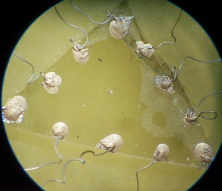
The sample of GaN can be produced by MOCVD or MBE. The interaction of the preparation of the GaN in MOCVD is: Ga(CH3)3+NH3--GaN+3CH4↑. The samples we are using now are the heterostructures of GaN/AlGaN, on a wafer of Sapphire. Metal contact can be prepared by levels of different metals. The Hall bar on the surface of the sample can be prepared using a dry-etching method, afterward the growth of gate is also necessary.

Dr. Rui-Rui Du
rrd@rice.edu
Rice University Physics & Astronomy
Dell Butcher Hall Rm. 170
1900 Rice Blvd. Ent. 20
Houston, TX 77005
>Office Phone: 1-713-348-5780
>Lab Phone/Fax: 1-713-348-5719